


German government sources have stated that while the global economy is expanding, it is...
Dubai, United Arab Emirates – April 16, 2024 (Newsfile Corp.) – Doric Blockchain, a...
German government sources have revealed that while the threat of a global recession has...
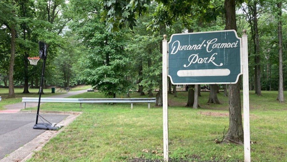
The township of Edison has announced plans to repair and upgrade sports courts at...
In recent news, Hydro has launched a new recycling unit at its Årdal primary...

On Monday, shares of Trump Media & Technology Group dropped by 18.4% after the...

The groundbreaking ceremony for the new Transportation Technology Center at the College of Southern...
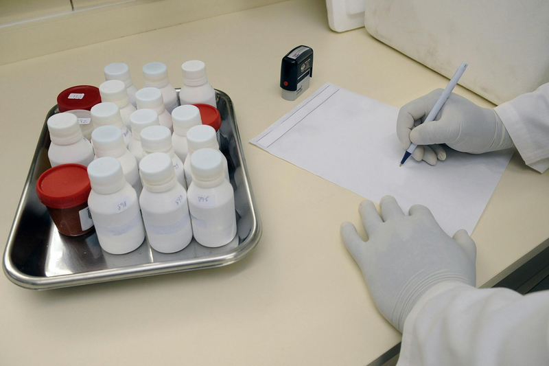
Isospec Analytics has secured $1.9M in funding to bring new technologies to market that...
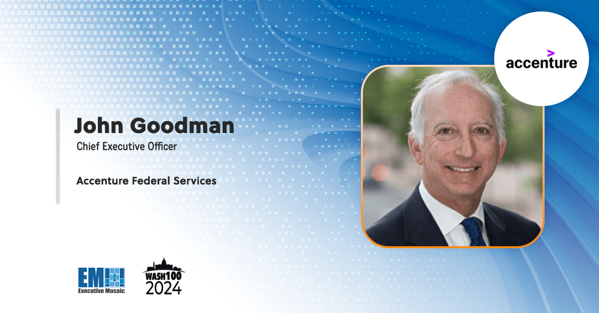
Cognosante, a provider of federal digital transformation and cloud modernization platforms, has been acquired...
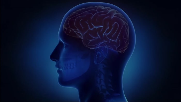
Taking care of your brain is vital for a productive and fulfilling life. The...